What do Hazelnuts, Cupcakes and Our Planet Have to Do With an Invisibility Cloak? Well, It’s All About Nanotechnology!
How would you feel if you had your own “invisibility cloak” just like our favourite child hero Harry Potter? Or if you were to own a smartphone as thin as a sheet of paper? Or, if your bulky camera bag became the size of a hand-held purse as your DSLR camera shrunk to one resembling the size of a fruit cake? I am sure that this sounds like science fiction to you, and you might be wondering whether it is at all possible in reality. Well, the truth is – some laboratories are at the brink of making this a reality soon. You still don’t believe this? Then follow me into the world of nanotechnology and metasurfaces – the two key players that make this dream possible!
How can we begin to imagine the size of one nanometer?
So what is nanotechnology? It is the science that deals with nanometer (nm) size objects. But how can we begin to imagine a nm-sized object? Let´s start with a cupcake. The size of a normal cupcake is around 5 cm, and an individual sprinkle on top of it is around 5 mm. To go even smaller, we can compare the sprinkle (5mm) with the thickness of a human hair, which is about 0.1 mm or 100 microns, measuring about 50 times smaller than a single sprinkle on top of the cupcake. Nanotechnology deals with structures which are 1000 times smaller than a single hair, i.e. about 0.1 micrometer or 100 nanometer– which is 50,000 times smaller than a sprinkle. In nanotechnology, the dimension of the structures can also measured be in tens of nanometer. It’s hard to picture this, so before we move on, let’s shift this scale back up to a more familiar format – imagine the hazelnut on top of our cupcake in comparison to our planet’s diameter – this is roughly like the size relation of one nanometer to one meter!
The cleanest research environment in the world
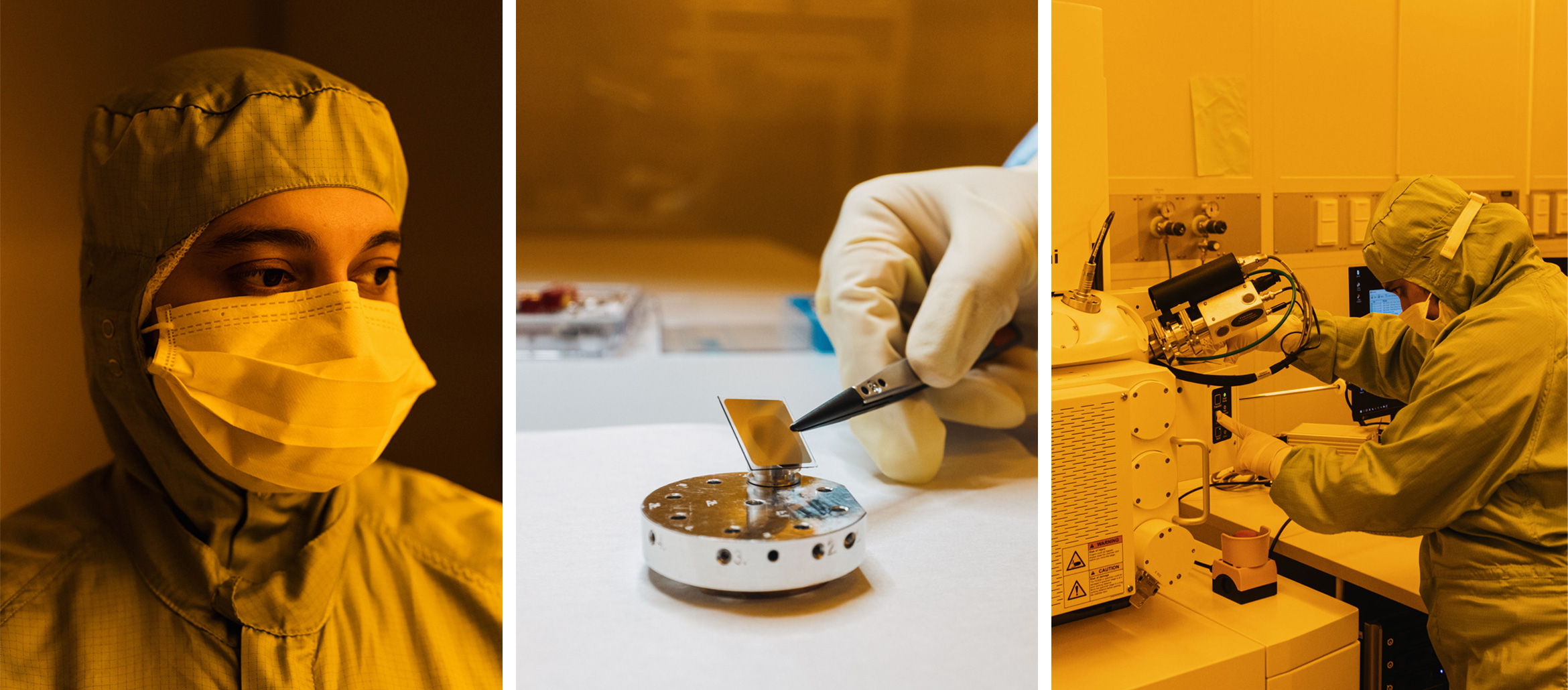
Can you believe that we can build objects with nanometer-sized particles? Yes, that is actually possible! But since nanotechnology deals with such small structures which are 100 times smaller than an average dust particle, special care needs to be taken to fabricate them. On a normal day the air around us usually contains around 1000 dust particles of sizes approximately ranging from 0.5 microns to 20 microns. Trying to put together nano particles in a normal room would be like trying to place a sprinkle on a cupcake while thousands of big apples per cubic meter are flying around you and hitting the surface of the icing. So to work with particles of nanometer size, we need special, extremely clean rooms where the air contains very few dust particles. These specialized places are, unsurprisingly, called ´cleanrooms´. Researchers who enter must cover themselves from head to toe, with only their eyes exposed to keep the room clean and dust free. Cleanrooms are also divided into several classes depending on the number of dust particles per cubic foot. There are, for example, ‘Class 100’ rooms that have 3520 particles of sizes greater than 0.5 micron per cubic meter, while for ‘Class 1000’ there can be up to 32500. It is in these cleanrooms that we have specialized machines with which we can fabricate nm sized objects!
So now that we understand where nanotechnology is being fabricated, let’s try and understand the next keyword- metasurface.
Do you want your cupcake icing with two or ten flavours, sprinkles and hazelnut pieces? – It’s all about combination and structure
Let´s again take the cupcake as our example and this time let’s concentrate on its icing. If we want to put 3 different icings on a standard cupcake, we would need sharper, more precise tools to apply the different components. The taste of this icing would be different too. Now, let´s imagine if we have very sharp tips available such that we can put 100 types of different icing on the same cupcake all at once. With such a cupcake, a normal human eye and tongue will not be able to distinguish the individual colours and flavours – but the resultant colour and flavour will be unique, rising from the micro-combination. Moreover, instead of choosing 100 different types of icing we can also choose 4 icings and repeat them hundreds of times in our desired manner and pattern. Depending on what icing we choose and how we arrange them each time, the cupcake would always taste different.
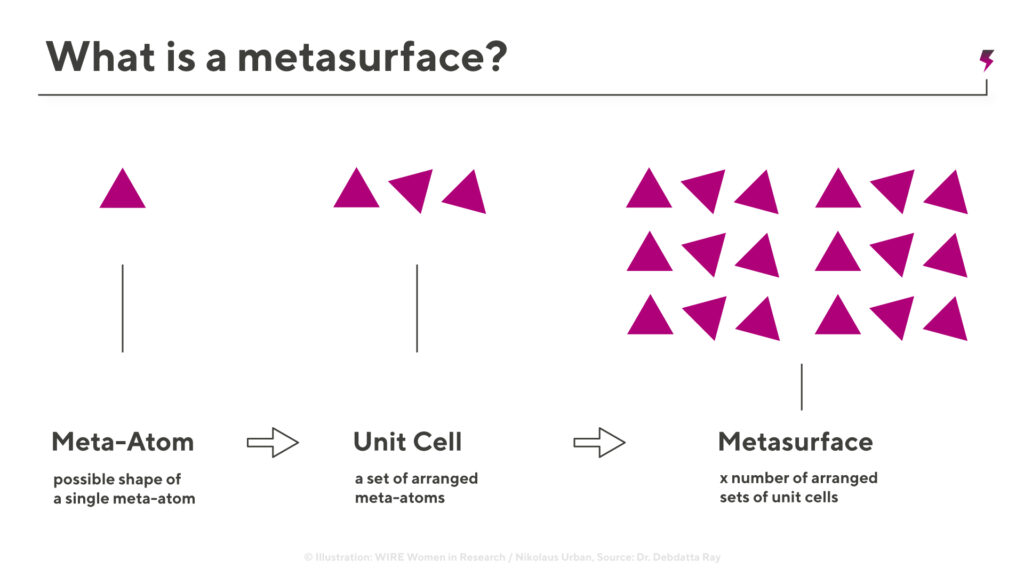
With the help of nanotechnology, scientists use this same principle to reduce the size of traditional optical devices and components such as lenses, mirrors, and prisms. We can make a unique surface called ´metasurface´ that consists of thousands of nm sized objects – made possible by nanotechnology.
How we can use nanostructures to generate various optical functions
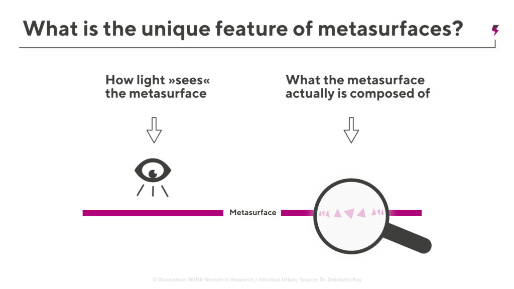
The resulting individual nanostructures are not “seen” by the light, rather the light encounters a singular unique surface encoded with thousands of tiny structures in a predefined manner. This encoding defines how the output light will behave and can combine several optical functions into one. This has been graphically explained in Figure. 1.1 and 1.2.
Due to the immense advances in nanotechnology, it is now possible to fabricate both simple and complicated shapes of dimensions consisting of several hundreds of nm. Since the function of the metasurface depends on the shape and the sizes of nanostructures, it is possible to mimic the functionality of almost all traditional optical components with the metasurface. This idea is already used to encode the functions of normal optical components.

We now have metasurfaces working as lenses and beam splitters that go into commercial cameras. Researchers are using metasurfaces to encode more complicated functions like the vector beam generator. A vector beam is a light beam that shows different polarizations at different parts of the detector plane. Such beams are very useful in optical trapping or in applications related to quantum like quantum entanglement. Since the nanostructures are very small and their thickness is in hundreds of nm, the resulting metasurface is only a few hundred microns thick. Thus, the resulting devices are drastically scaled down in dimension. Moreover, this metasurface can also be made of different materials or of one material allowing a plethora of combinations – remember the icing on the cupcake!

So how are these metasurfaces generally made?
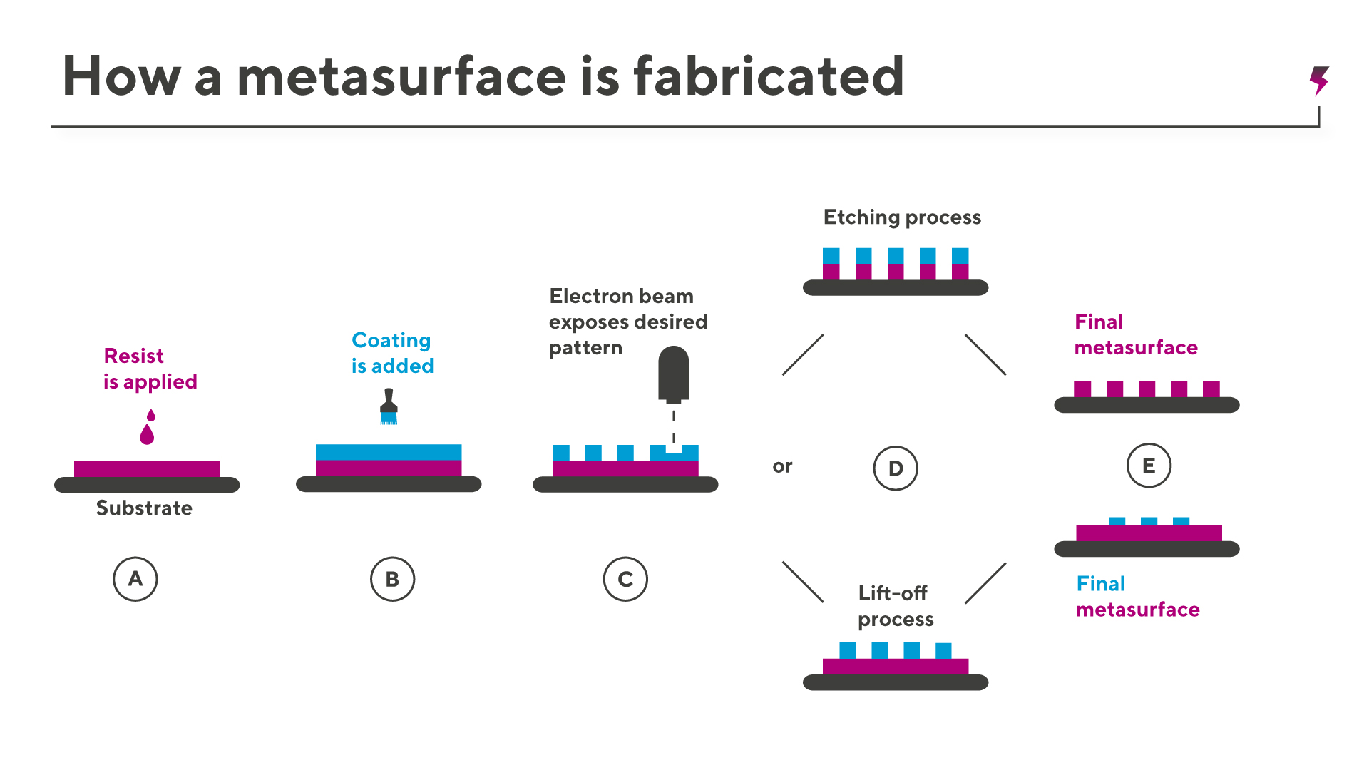
As mentioned before, in order to create these metasurfaces we need cleanrooms and specialized machines. One of the key steps that determines the size of the nanostructures in the metasurface is called “lithography”. In order to perform this lithography, we have specialized machines called electron beam lithography machines. In this machine, a beam of electrons comes and strikes the surface (also called “substrate”) on which the metasurface is going to be made. Before applying lithography, this surface needs to be coated with a material called “resist” (See step B in Figure 2). This material will react with the electron beams. After this step, the substrate along with the resist is treated with special chemicals (Step D in Figure 2) – a process called “development”.
After the electron beam lithography process, the resist is exposed on certain parts where the electrons have interacted with the resist while on other parts the resist remains unchanged where no electrons have interacted. During the development process the sample is immersed in a chemical called the “developer” which only selectively attacks the exposed parts of the resist. For the positive resist this chemical washes away the exposed part i.e. after development the exposed part will no longer have the resist while the unexposed part will still have the resist (as shown in Step D in Figure 2). For the negative resist the opposite happens, here the developer washes away the unexposed part of the resist while the exposed part of the resist stays. This development process is crucial in nanofabrication as it decides the dimensions of the nanostructures.
This step of electron beam lithography along with development is crucial to determine the sizes of the nanoparticles. After this step, depending on what the material or desired end result is, there are two main approaches: for metals, the lift-off approach is generally used while for dielectrics (i.e. inslulating material which does not conduct an electric current), the etching process is used. However, both these processes can also be used in tandem for advanced metasurfaces, e.g for metasurfaces using both metal and dielectric nanostructures. In metasurface fabrication, lithography is not the only step that uses machines, the etching step also requires very advanced machines as well .

Metasurfaces – Tiny surfaces, giant impact!
So now that we have a brief idea as to what metasurfaces are and how are they made, let´s begin to understand how these metasurfaces are relevant and why we should be interested in them.
As explained previously, metasurfaces mimic the functions of bulky optical components. Thus the success of metasurface will miniaturise all these components, leading to smaller cameras and sleeker, more compact optical components.
In academic research, there have already been several successful optical applications of metasurfaces. Some of the important ones among them are digital holography (for different incident light with different polarizations, the output will be different holograms), beam splitters, or generation of higher order optical beams. Moreover, metasurface can also be used in bio-sensing.
Slowly, the field of metasurface is also finding immense relevance in commercial products. Several startups, as well as longer-established companies are very much interested in paving the way for metasurfaces in commercialization. Metasurfaces have already been commercially incorporated in lenses and as anti-reflective coatings. They have also been used in security as well. Several key companies are working to incorporate them more in the lens system, thus reducing the size of their products.
The research on metasurfaces will help us to introduce a world of sleeker technological components. The day is not far when we can sneak out at night easily with our own invisibility cloak, or can put our expensive mini-DSLR in our fashionable handbags!!
